|
|
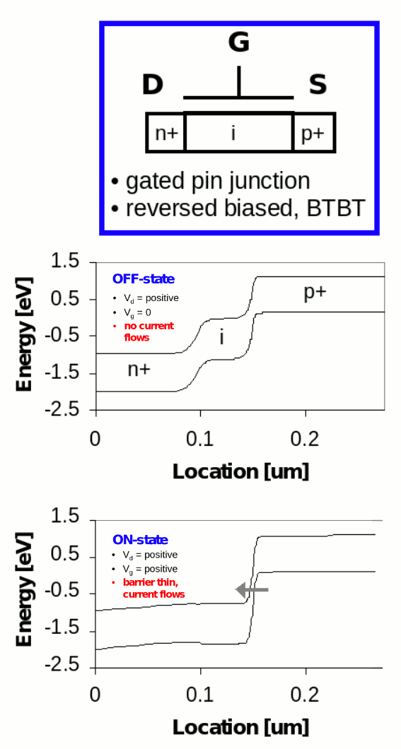
| Fig. 1: Top: Schematic of a tunnel transistor (TFET) architecture; Bottom: Energy band diagram illustrating the TFET ON and OFF state conditions. |
The Schrödinger formulation of quantum mechanics presents an interesting phenomenon where a particle tunnels through an energy barrier, similar to evanescent wave coupling of electromagnetic waves. One interpretation of this duality involves the Heisenberg uncertainty principle, which defines a limit on how precisely the position and the momentum of a particle can be known at the same time. This implies that there are no solutions with a probability of exactly zero (or one). Hence, the probability of a given particle's existence on the opposite side of an intervening barrier is non-zero, and such particles will appear - with no indication of physically transiting the barrier - on the 'other' side with a frequency proportional to this probability.
In TFETs tunneling of interest is band-to-band tunneling. For band-to-band tunneling to occur, an electron in the valence band of semiconductor tunnels across the band gap to the conduction band without the assistance of traps. The band gap acts as the potential barrier that the particle tunnels across. An electron travels from the valance band to the conduction band without the absorption or emission of photon in direct tunneling. A tunneling particle acquires a change in momentum by absorbing or emitting a phonon in the indirect tunneling process. In indirect semiconductors whose gamma-centered direct band gap EΓ, is much greater than their indirect band gap, EG indirect tunneling is the main tunneling process. The direct tunneling process is negligible in indirect band gap materials like silicon because the transmission probability decreases rapidly with increasing barrier height. The electron tunneling through the band gap is akin to particle tunneling through a potential barrier, and the most probable tunneling path the smallest barrier. For direct tunneling, the requirement for conservation of perpendicular momentum causes an increase in the tunneling. A particle with some perpendicular momentum in the valence band must tunnel to state with the same perpendicular momentum in the conduction band, which results in a longer tunneling path. In the indirect tunneling process, the phonon does impart or absorb a change in the momentum of the particle. Therefore, the electron, phonon interaction of the indirect tunneling process decouples the perpendicular momentum of valence band and conduction band. An electron in the valence band can tunnel to any state in the conduction band such that energy and perpendicular momentum are conserved:
 |
(1) |
 |
Where β is the wave vector of the phonon. Under the continuum approximation, β can be any value so that kc⊥ is independent of kv⊥. However, the energy imparted for a momentum transfer from Γ-valley maximum to the X-valley minimum by a transverse acoustic phonon is approximately 18 meV. [1] Because this energy is quite small, the approximation is made that no change in total energy occurs with the phonon interaction, and the term ℏωβ is neglected. In field effect transistors, tunnelling occurs with barriers of thickness around 1-3 nm and smaller in which the gate is controlled via quantum tunnelling rather than by thermal injection, reducing gate voltage from ∼1 volt to 0.2 volts and reducing power consumption by up to 100x. If these transistors can be scaled up into VLSI chips, they will significantly improve the performance per power of integrated circuits.
The tunnel field-effect transistor (TFET) belongs to the family of so-called steep-slope devices that are currently being investigated for ultra-low-power electronic applications. [2] A key feature of the TFET, which is critical for low-power switching, is the possibility for an inverse sub threshold slope, S, below the limit of 60 mV/dec for normal FETs. [3]
 |
(2) |
The fundamental challenge for realizing commercially competitive TFETs is a limited on-current level, which is typically addressed by creating higher doping levels and abrupt doping profiles. [4] Fig. 1 shows a schematic of an n-channel TFET architecture which incorporates a highly doped p+ source region, a near intrinsic channel region and n+ drain region.
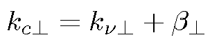
TFET is simply a gated p-i-n diode, which is operating under reverse bias condition. In a MOSFET the source of carrier injection mechanism is thermal injection but a TFET utilizes band-to-band tunneling as a source carrier injection mechanism. Fig. 1 shows the band diagrams of the n-channel TFET in the OFF and ON states. In the OFF state, there is a wide potential barrier between the source and the channel, as a result no tunneling is occurring. Only a very small leakage current exists. But when the gate voltage exceeds the threshold voltage, the potential barrier between the channel and the source becomes narrow enough to allow a significant tunneling current, which is called ON state. Because of the different source carrier injection mechanism in the TFET compare to a MOSFET, it can achieve sub-60-mV/dec S (where S is the sub threshold slope) [3]. Wang et al. [5] showed the feasibility of the TFET for low-power applications; some interesting studies have been reported. Zhang et al. [6] provided a theoretical analysis that the S value of TFETs can be reduced below 60 mV/dec.
TFET is an ambipolar device, it will show p-type
behavior with dominant hole conduction and n-type behavior with dominant
electron conduction. But this ambipolarity can be suppressed by
designing an asymmetry in the doping level or profile, or by restricting
the movement of one type of charge carrier using Heterostructures. In
principle, because of the asymmetry TFETs can achieve much higher
ION-IOFF ratio over a given gate voltage swing
compared to the MOSFETs, making the TFET architecture an attractive
vehicle to implement low supply voltage (V
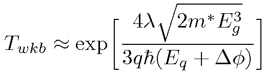
A conductive channel opens as soon as the channel valence band has been lifted above the source conduction band because carriers can now tunnel into empty states of the channel. Because only carriers in the energy window ΔΦ can tunnel into the channel, the energy distribution of carriers from the source is limited; the high-energy part of the source Fermi distribution is effectively cut off, as shown in Fig. 2 (left). Thus the electronic system is effectively 'cooled down', acting as a conventional MOSFET at a lower temperature. This filtering function is the reason why we are able to achieve an S of below 60mV per decade (Fig. 2 right). However, the channel valence band can be lifted by a small change in gate voltage, and the tunneling width can effectively be reduced by the gate voltage. S in a TFET is not constant, As a consequence of the BTBT mechanism, but it depends on the applied gate-source bias, as indicated in Fig. 2 (right), increasing with the gate-to-source bias. In a TFET S remains below 60 mV per decade over several orders of magnitude of drain current and that's why you have a better voltage scaling of a TFET than a MOSFET. One challenge in TFETs is to realize high on currents because ION critically depends on the transmission probability, TWKB, of the inter band tunnelling barrier. This barrier can be approximated by a triangular potential, as indicated by the grey shading in Fig. 2 (left), so T can be calculated using the Wentzel-Kramers-Brillouin (WKB) approximation:
 |
(3) |
Where m* is the effective mass and Eg is the bandgap. Here, λ is the screening tunnelling length and describes the spatial extent of the transition region at the source-channel interface; it depends on the specific device geometry. In a TFET, at constant drain voltage, VD, the VG increase reduces λ and increases the energetic difference between the conduction band in the source and the valence band in the channel (ΔΦ), so that in a first approximation the drain current is a super exponential function of VG. As a result, in contrast to the MOSFET, the point subthreshold swing of the TFET is no longer a constant but strongly depends on VG. The smallest subthermal values occur at the lowest gate voltages. A high on current requires a high transparency of the tunnelling barrier, thus maximizing TWKB, which in the best case should be unity. Eqn. (3) suggests optimized design approaches to boost the on current. WKB approximation works properly in direct bandgap semiconductors, such as InAs, but has limited accuracy for Si and Ge structures or when quantum effects and phonon assisted tunnelling become dominant.
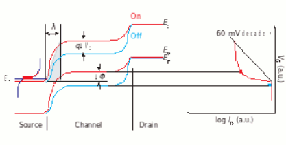 |
| Fig. 2: Left: Schematic energy band profile for the off state (dashed blue lines) and the on state (red lines) in a p-type TFET. In the on state electrons in the energy window, ΔΦ (green shading), can tunnel from the source conduction band into the channel valence band. Electrons in the tail of the Fermi distribution cannot tunnel because no empty states are available in the channel at their energy (dotted black line), so a slope of less than 60 mV decade can be achieved. [7] |
The goals for TFET optimization are to simultaneously achieve the highest possible ION, the lowest Savg over many orders of magnitude of drain current, and the lowest possible IOFF. To outperform CMOS transistors, the target parameters for TFETs are: ION in the range of hundreds of milliamperes; Savg far below 60 mV per decade for five decades of current; ION/IOFF > 105; and VDD < 0.5 V. Because S decreases with the VG, TFETs are naturally optimized for low-voltage operation. To realize a high tunnelling current and a steep slope, the transmission probability of the source tunnelling barrier should become close to unity for a small change in VG. The WKB approximation suggests that the bandgap (Eg), the effective carrier mass (m*) and the screening tunnelling length (λ) should be minimized for high barrier transparency. Whereas Eg and m* depend solely on the material system, λ is strongly influenced by several parameters, such as the device geometry, dimensions, doping profiles and gate capacitance. A small λ results in a strong modulation of the channel bands by the gate. This requires a high-permittivity (high K) gate dielectric with as low an equivalent oxide thickness as possible. Furthermore, the body thickness of the channel should be minimized, showing in the best case one-dimensional electronic transport behavior. The abruptness of the doping profile at the tunnel junction is also important. To minimize the tunnelling barrier, the high source doping level must fall off to the intrinsic channel in as short a width as possible. This requires a change in the doping concentration of about 4-5 orders of magnitude within a distance of only a few nanometres. Increasing the source doping reduces λ and may lead to a slightly smaller energy barrier at the tunnel junction because of bandgap narrowing. However, the energy filtering effect described above becomes effective only if the Fermi energy in the source is not too large. [7]
In an integrated DG-CMOS/DG-Tunnel-FET process, the Tunnel FETs will benefit from the added gate, such that the current will be at least doubled. In this way, the ON-current is boosted, while the OFF-current, still in the femtoamperes or picoamperes range, increases by the same factor but remains extremely low. It is worth noting that, for ultrathin siliconon-insulator (SOI) MOSFETs, some reports suggest that this improvement can be even higher when volume inversion takes place. [8]
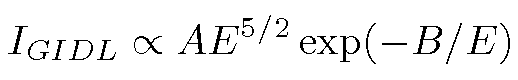
The temperature and voltage dependence of the GIDL effect in MOSFETs under low electric field is investigated. The dependency of the GIDL current on the electric field E can be expressed as
 |
(4) |
The parameter are given by A ∝ EG-7/4 and B ∝ EG3/2, with the band-gap energy EG. From Eqn. (4) the GIDL current is derived to be very weak dependent on the temperature. However a second effect exists at low electric field. Under low electric field the GIDL current can be described by the Shockley-Read-Hall (SRH) model, which has strong temperature dependence. Under higher electric field the GIDL current is dominated by Band-to-Band tunneling which has weak temperature dependence. Due to the comparable physical principle of the GIDL current and the TFET, Eqn. (4) can be used to separate the SRH part of the TFET characteristic from the Band-to-Band tunneling part. Hence, starting from a gate-to-source voltage of approximately -1V the Band-to-Band tunneling is the dominant mechanism. Like for the MOSFET the temperature dependency is changing with the voltage applied. For the MOSFET the zero temperature coefficient point can be used for digital circuit design to make the system performance independent of the temperature. For the TFET the voltage where the change of the temperature dependence occurs is outside the useable range. Hence, the combination of the MOSFET and the TFET can be used to compensate for temperature effects. For analog circuits the temperature dependence has to be verified in more detail. Obviously, the temperature effect of the TFET is more comparable to the bipolar device. This may allow novel topologies for a "band-gap"-like voltage reference circuit. [9]
An improved on-current and decreased subthreshold swing can be obtained by the careful choice of a gate dielectric. Kathy Boucart Et al. compared 3 nm physical thickness of Si3N4 and two high-k dielectrics with dielectric constants of 21 and 29 with SiO2. In addition to improved Ion, both the point and average subthreshold swing improve as the result of the better gate coupling given by a high-k dielectric. The off current is less than 1 fA for all materials. The on-current of a Tunnel FET does not increase merely proportionally to the increase in the gate capacitance, as it would for a conventional MOSFET. Their numerical simulation shows the Tunnel FETs subthreshold swing continues to improve as the gate dielectric permittivity increases. The swing for the conventional MOSFET hits its 60 mV/decade limit at room temperature and cannot improve further. While high-k dielectrics have advantages for device characteristics, when put directly in contact with a silicon channel, they can lead to defects at the semiconductor/dielectric interface. Although Tunnel FETs might be less sensitive to changes in channel mobility than MOSFETs since the transport through the tunnel junction dominates over any scattering in the channel, standard CMOS fabrication techniques require an interfacial layer between the high-k dielectric and the silicon channel. High-k dielectrics bring additional challenges such as the limitations of soft and hard dielectric breakdown. Depending on the characteristics of fabricated high-k dielectric layers, it may be necessary to limit applied gate voltages. [10]
Today TFETs represent the most promising steep-slope switch candidate, having the potential to use a supply voltage significantly below 0.5 V and thereby offering significant power dissipation savings. Because of their low off currents, they are ideally suited for low-power and low-standby-power logic applications operating at moderate frequencies. Other promising applications of TFETs include ultralow-power specialized analog integrated circuits with improved temperature stability and low-power SRAM.
The biggest challenge is to achieve high performance (high ION) without degrading IOFF, combined with an S of less than 60 mV per decade over more than four decades of drain current. This requires the additive combination of the many technology boosters which are available or under research.
© Rahim Esfandyarpour. The author grants permission to copy, distribute and display this work in unaltered form, with attribution to the author, for noncommercial purposes only. All other rights, including commercial rights, are reserved to the author.
[1] H. Holonyak, Jr. et al., "Direct Observation of Phonons During Tunneling in Narrow Junction Diodes." Phys. Rev. Lett. 3, 167 (1959).
[2] B. Ganjipour et al., "Tunnel Field-ffect Transistors Based on InP-GaAs Heterostructure Nanowires," ACS Nano 6, 3109 (2012).
[3] W. Y. Choi et al., "Tunneling Field effect Transistors (TFETs) with Subthreshold Swing (SS) Less Than 60 mV/dec", IEEE Electron Device Lett. 28, 743 (2007).
[4] J. I. Pankove, Optical Processes in Semiconductors (Dover, 2010).
[5] P.-F. Wang et al., "Complementary Tunneling Transistor for Low Power Applications," Solid State Electron. 48, 2881 (2004).
[6] Q. Zhang, W. Zhao and A. Seabaugh, "Low-Subthreshold-Swing Tunnel Transistors," IEEE Electron Device Lett. 27, 297 (2006).
[7] A. M. Ionescu and H. Riel, "Tunnel Field-Effect Transistors as Energy-Efficient Electronic Switches", Nature 479, 329 (2011).
[8] F. Balestra et al., "Double-Gate Silicon-on-Insulator Transistor With Volume Inversion: A New Device With Greatly Enhanced Performance," IEEE Electron Device Lett. 8, 410 (1987).
[9] T. Nirschi et al., "The Tunneling Field Effect Transistor (TFET): The Temperature Dependence, the Simulation Model, and Its Application," Proc. Intl. Symp. on Circuits and Systems ICAS 3, 713 (2004).
[10] K. Boucart and A. M Ionescu, "Double-Gate Tunnel FET With High-κ Gate Dielectric," IEEE Trans. Elect. Dev. 54, 1725 (2007).