|
|
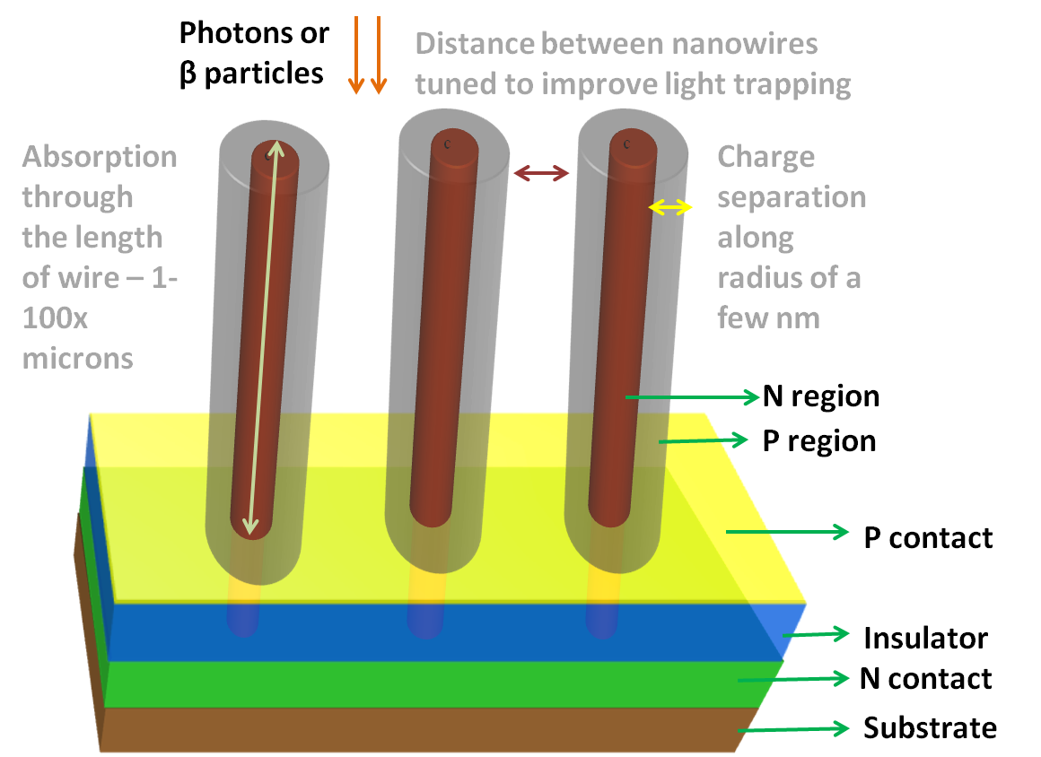
| Fig. 1: Proposed configuration of a nanowire solar cell/beta-cell. |
Natural radioactivity produces radiation that has energy. Atomic/Nuclear Batteries harness this energy. Quantitative first principles that enable this and the types of conversion are discussed elsewhere. [1-2] This document proposes improvements in design of direct and indirect conversion nuclear batteries
Direct conversion nuclear batteries are identical to solar cells in their operation, except that they use high energy particles from radiation instead of photons. We come across improvements in direct conversion nuclear batteries that use beta decay (beta-cells) by tweaking the diode structure (e.g.: using III-V materials, using p-i-n junctions), including mechanisms and structures for light trapping and preventing reflections, using 3D geometries for light trapping and building beta- cells in porous silicon. [3-5] These methods of improving beta-cells are very similar to the ways in which the improvement of solar cells occurred. [6] Solar cells went the nanowires route after these improvements were made, [7] although the solar cell community has yet to make full use of carbon nanotubes, as it has done with nanowires, despite some efforts. [8-9] Likewise, going the route of nanowires and nanotubes would improve the performance of beta-cells as nanowires did to solar cells.
Typically, nanowires are used in a vertical configuration, as shown in Fig. 1. The main advantages of using nanowires in this configuration are: (i) reduced reflection of incident particles or photons due to tapered refractive index, (ii) improved carrier collection because of radial extraction throughout the length, (iii) possibility of band structure tuning which reduces losses due to phonons and heat, and (iv) confinement of carriers in 1D, which could yield better transport. Some issues include surface impurities that degrade transport, as well as fabrication issues (i.e. conformal coating of the subsequent layers).
Since the beta particles have far higher energy than photons, the beta-cell, unlike solar cells, must be designed so that the outer layer of the nanowires (generally p-type layer) is able to collect the thousands of excess electrons generated by each beta particle, and simultaneously be able to withstand large amounts of damage caused by the high energy impact. An alternative could be to fill in the space between the nanowires with radio luminescent substances like phosphor, protect the nanowires from beta particles, and use the light that phosphor emits upon impact to drive nanowire-based diodes. In this configuration, we can use low quality semiconductors that have a small diffusion length since the charge separation is along the radius of a few nm or more, or we could use a small bandgap material with very high electron mobility such as InSb. [10] In solar cells, similar configurations based on nanotubes have not yet been shown to outperform nanowires.
This configuration is extremely hard to fabricate with nanotubes since they have very small diameter and no substantial distinction between the 'core'and the surface of the nanotube, unlike that of p-n diode nanowires. It is also difficult to achieve the structural configuration of a nanowire array, which is tunable. Efforts in Refs. [8-9], however, show that it is possible to take this approach. Multi walled nanotubes (MWNTs), and specifically double walled nanotubes (DWNTs), can have distinct inner and outer walls that can be individually doped. [11-12] The lengths of these can be up to a few hundreds of microns, while the spacing is mainly determined by the nature of the walls, with little influence by the growth conditions once the 'crowding effect' takes over and it is in the order of the diameter. [13] These smaller dimensions could be better for 'photonic crystal light trapping' of beta particles which have a smaller de-Broglie wavelength when compared to photons. Additionally, charge separation needs to occur within the small distance between the nanotube walls. Electron-hole pairs move as excitons because of their strong coupling in nanotubes. By fluorescence quenching, the exciton diffusion lengths can be reduced to the order of the distance between the walls. [14] The contacts to the two walls can be made with metals of different work functions, such that the band offsets allow only electrons to be collected from the n-type and holes from the p-type materials; thus, we could prevent shorting of the contacts even if they are in the physical vicinity of each other.
Thus, we could take leads from the history of solar cells, but tread a route the solar cell community is unlikely to follow.
© Suhas Kumar. The author grants permission to copy, distribute and display this work in unaltered form, with attribution to the author, for noncommercial purposes only. All other rights, including commercial rights, are reserved to the author.
[1] S. Kumar, "Energy from Radioactivity," Physics 240, Stanford University, Fall 2011.
[2] S. Kumar, "Types of Nuclear/Atomic Batteries," Physics 241, Stanford University, Winter 2012.
[3] K. E. Bower et al., Polymers, Phosphors, and Voltaics for Radioisotope Microbatteries (CRC Press, 2002).
[4] W. Sun et al., "A Three-Dimensional Porous Silicon p-n Diode for Betavoltaics and Photovoltaics," Adv. Mat. 17, 1230 (2005).
[5] B. Liu et al., "Power-Scaling Performance of a Three-Dimensional Tritium Betavoltaic Diode," Appl. Phys. Lett. 95, 233112 (2009).
[6] A. Luque and S. Hegedus, Handbook of Photovoltaic Science and Engineering (Wiley, 2011).
[7] E. C. Garnett et al., "Nanowire Solar Cells," Annu. Rev. Mat. Res. 41, 269 (2011).
[8] A. Kongkanand, R. M. Dominguez and P. V. Kamat, "Single Wall Carbon Nanotube Scaffolds for Photoelectrochemical Solar Cells: Capture and Transport of Photogenerated Electrons," Nano Lett. 7, 676 (2007).
[9] J. Wei et al., "Double-Walled Carbon Nanotube Solar Cells," Nano Lett. 7, 2317 (2007).
[10] D. L. Pulfrey, Understanding Modern Transistors and Diodes (Cambridge U. Press, 2010).
[11] F. Villalpando-Paez et al., "Raman Spectroscopy Study of Isolated Double-Walled Carbon Nanotubes with Different Metallic and Semiconducting Configurations," Nano Lett. 8, 3879 (2008).
[12] G. Chen et al., "Chemically Doped Double-Walled Carbon Nanotubes: Cylindrical Molecular Capacitors," Phys. Rev. Lett. 90, 257403 (2003).
[13] S. Reich, C. Thomsen and J. Maultzsch, Carbon Nanotubes: Basic Concepts and Physical Properties (Wiley-VCH, 2004).
[14] L. Luer et al., "Size and Mobility of Excitons in (6, 5) Carbon Nanotubes," Nature Phys. 5, 54 (2009).