|
|
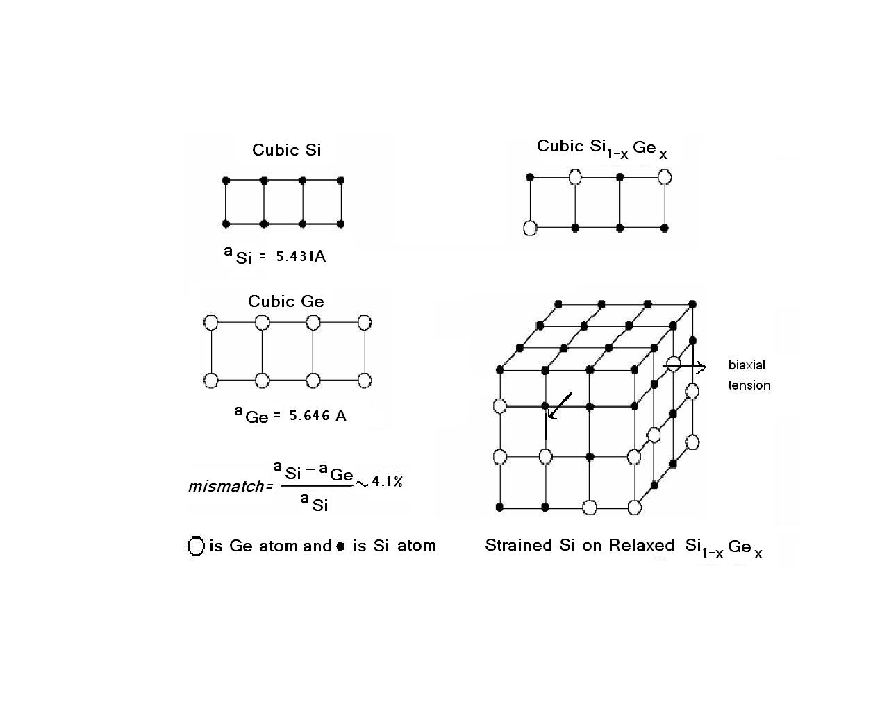
| Fig. 1: Biaxial tensile strain generation by Si epitaxy growth on SiGe. |
Strain is a state-to-art technology in today's transistors of integrated circuits. This article will make a simply physical analysis of the strained induced conductivity, or to say, effective mobility enhancement in both n- and p-type silicon by using biaxial tensile strain as an example.
Many techniques can be used to generate strain for Silicon. The normally used technology to generate biaxial tensile strain is to grow a silicon epitaxy layer on relaxed SiGe. Because the silicon epitaxy has to match the lattice structure of the SiGe substrate, it will have the same lattice constant as the SiGe substrate. We know the natural lattice constant of Si is less than SiGe, so the Si epitaxy layer will be forced to "expend" on the surface plane of SiGe substrate. This will introduce a biaxial tensile strain for the Si layer. Fig 1 shows this strain generation technology.
Under low fields, the current in doped n/p-type semiconductor is directly proportional to the electric field, so we have Ohm's law. Assuming it is n-type Silicon and the electric field applies in the z direction, then the current flows in z direction. Then:
|
| Fig. 2: Constant energy surface for silicon conduction band. |
Jnz is current density, n is the number of electrons per volume in silicon, q is the charge of a single electron, Ez is the electric field, and μn is what we call mobility of electrons. It is given by

where τ is a constant, called the average relaxation time and m* is the transport effective mass. It depends on the transport direction. It is different from the band effective mass, although they are related. The conductivity is thus
|
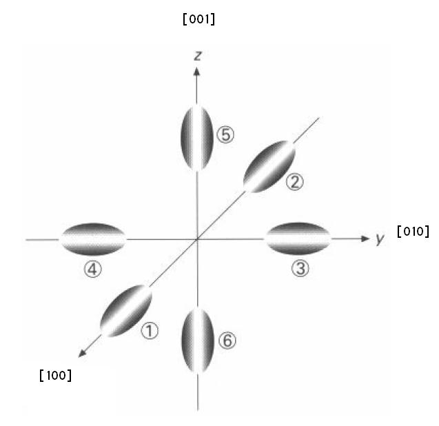
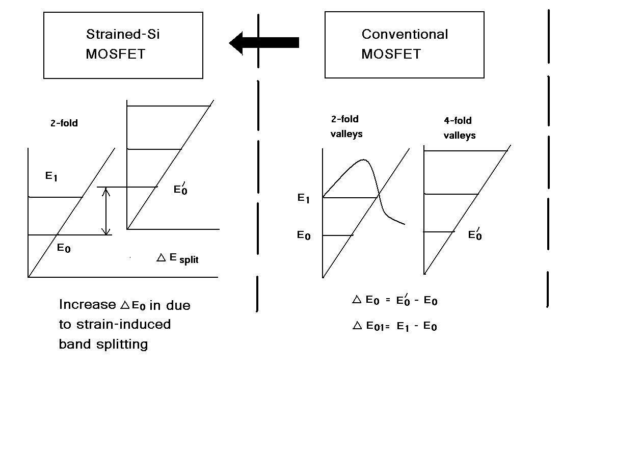
| Fig. 3: Biaxial tensile strain in the x-y plane induced silicon conduction band splitting for electrons under z-direction confinement. |
The silicon conduction band has six equivalent valleys in E-k space (Fig. 1). Each is an ellipsoid. The dispersion relation for electrons in one of the [100] valleys is
where k is the wave vector, ECO is a constant potential energy, ml* = 0.916 m0 and mt* = 0.019 m0 are the longitudinal and transverse effective masses, respectively. (m0 is the free electron mass.) Because of symmetry, the dispersion relation for the other 5 valleys can be achieved by rearrangement of the masses.
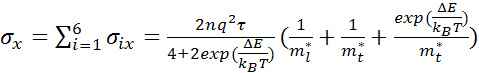
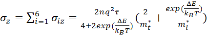
If there is no strain on Silicon, the six equivalent valences are equally populated by electrons, so the conductance in the x, y and z directions is the same. For the x-direction, for example, we have
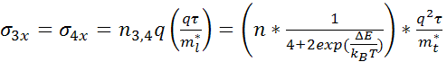
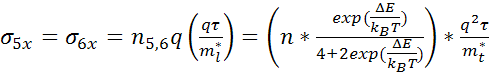
If, on the other hand, we apply biaxial tensile strain for Silicon in the x-y plane or compressive strain in the z direction, the six [100] minima are no longer degenerate. The two minima in the z-direction are lower in energy by an amount ΔE compared to those in the x and y direction. This is shown in Fig. 3. The total electron population remains constant but each ellipsoid will get a weighted proportion of the carriers depending on its energy. If we assume that the silicon is non-degenerate, so that electrons in the conduction band obey Boltzmann statistics, and that the current is in x direction, we obtain
 |
 |
 |
 |
The same is the case for currents in the y-direction. For the z-direction we have
|
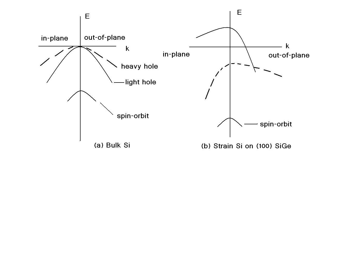
| Fig. 4: Valence band changes induced in silicon by biaxial stress in the x-y plane. |
If ΔE is big enough, which means the strain is large enough, we have
 |
 |
Without strain we have
So we can see conductivity in x or y direction is greatly enhanced with strain than without strain. If we make an electronic device with strain and let current flow in the X or Y device, we can get much larger current with the same voltage bias. This is the state-to-art technology for modern NMOS transistors in integrated circuits. I must note that the suppression of interband scattering by energy band splitting using strain also contributes to relaxation time increase and then mobility and conductivity enhancement. But for simplification, I did not include this in the above discussion.
The strain technique for hole mobility enhancement, which is used in P type silicon devices, especially PMOS transistor now uses the same principle as N type silicon we discussed above. The principle is to split sub-bands in energy and then let carriers to populate in low energy sub-bands. Fig 4 shows the change of valence bands by using biaxial tensile strain in a plane. With strain, besides sub-bands splitting, the shape of the sub-bands also changed, which is different from conduction band. Now both in-plane and out-of-plane hole mobility is improved, but it is mainly due to the reduced interband and intraband scatterings by lifting of the degeneracy between light- and heavy-hole bands and lowering of the spin-off band, not the reduction of the effective transportation mass as in the N type silicon case. So if we make a PMOS with biaxial tensile strain in a plane, we can thus enhance its conductivity.
© 2007 Xiao Zhang. The author grants permission to copy, distribute and display this work in unaltered form, with attribution to the author, for noncommercial purposes only. All other rights, including commercial rights, are reserved to the author.
[1] Mark Lundstrom, Fundamentals of carrier transport (Cambridge, 2000).
[2] L. Ye, Semiconductor Physics (Chinese Advanced Education, 1994).
[3] S. Takagi, IEDM Tech. Dig. [Proceedings of the 1997 International Electron Devices Meeting, Washington, D.C.] (IEEE,1997), p. 219.
[4] D. K.Nayak, Appl. Phys. Lett. 64, 19 (1994).