|
|
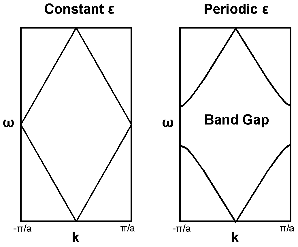
| Fig. 1: Prototypical 1D Band Gap Formation. |
Photonic crystal design revolves around one characteristic common to nearly all man-made photonic crystals – the photonic band gap. The photonic band gap (PBG) is defined as the range of frequencies for which no real, propagating solutions to Maxwell’s equations exist inside the photonic crystal. In other words, the photonic crystal reflects light within the bandgap extremely efficiently. Dielectric mirror coatings are well-known examples of one dimensional photonic crystals that exhibit a photonic band gap.
The existence of a photonic band gap is highly analogous to the semiconductor band gap commonly studied in solid state physics. To understand the basic principles which lead to its existence, we begin by considering a one dimensional system with a constant ε. For such a system, Schrodinger’s equation may be solved without incident to yield the well known free particle solution E(x) ~ eikx . We observe that ε may be considered to have a trivial periodicity A for all A > 0. Consequently we can rewrite the solution in the form E(x) ~ einπx/A . This solution has the dispersion relation shown in the first plot of figure 1. However, when ε is perturbed so that its periodicity is now non-trivially A, the degeneracy is broken and an important variational principle comes into play.
Specifically, as a consequence of Maxwell’s equations, it can be shown that the eigenvalues of the system satisfy the following relation:
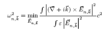
where the nth eigenfunction, En,k, is orthogonal to the lower n - 1 eigenfunctions. [3] The electric field will tend to minimize the eigenvalues by concentrating in high ε regions in order to maximize the denominator. [2] However, the orthogonality condition imposed on the eigenfunctions will increasingly force the higher eigenfunctions into the low ε regions. This "gap" between the eigenfunctions corresponds to the observed photonic band gap.
As one would expect from the above reasoning, the gap becomes more sizable as the contrast between the different ε regions is heightened. Consequently, a common technique in photonic crystal design is to either lower the ε of the low-ε regions or raise the ε of the high-ε regions in order to make the gap more observable. Usually, the extent to which this is done is limited by the materials available. A typical ε contrast usually hovers between 3:1 and 4:1. [3]
Another important factor that comes into play relates to the tendency of the electric field to concentrate in regions of high &sepsilon;, and how the geometry of the crystal can be made to facilitate this. In particular, when moving from a high-ε region to a low-ε region, ε |E|2, the "inverse potential" as Johnson calls it, decreases discontinuously if the electric field is parallel to the interface, and increases discontinuously if the electric field is perpendicular to the interface. [2] As a direct consequence of this, the band gap shrinks if the eigenfunctions of the electric field are perpendicular to the interface between the high and low dielectrics. To avoid this situation, the optimal crystal design should have the high dielectric regions consist of thin, vein-like structures which will cause the electric field to be parallel to the interface. This is almost precisely the blueprint employed by the photonic crystal with largest band gap yet discovered. [1]
However, practical considerations dictate which crystals can actually be fabricated. So while vein-like structures might possess the largest band gaps, the relative difficulty involved in their actual construction generally leads designers to typically rely on other heuristics.
Lattice symmetry is perhaps the most important consideration when designing a crystal. Specifically, it is desirable that the lattice periodicity be nearly identical in all directions. In reciprocal space, this translates to having a nearly spherical Brillouin zone so that the photonic band gap is equally large in any particular direction. This guarantees that if a band gap exists, it will be complete. Consequently, almost all photonic crystals with sizable band gaps are constructed from either hexagonal or diamond lattices. In fact, the top twenty photonic band gaps correspond to crystals based off the diamond morphology. [4]
While the preceding design considerations are essential towards devising a crystal with a sizable PBG, simulation is the test by fire of any given design. With the tremendous increase in computational power in recent years, finite difference time domain simulation (FDTD) is one of the leading methods of modeling a photonic crystal. It is also very simple to understand.
FDTD simulations work off the basic principle that the solution of any given partial differential equation may be approximated through a discretization of all relevant terms. This discretization implicitly assumes that all the functions involved may be expanded into Taylor series which may be then truncated to the desired order of accuracy. Thus, all partial derivatives become finite differences and all integrals become running sums. Then, the physical situation is modeled with some discrete user-specified spatial step size across some discrete user-specified temporal step size.
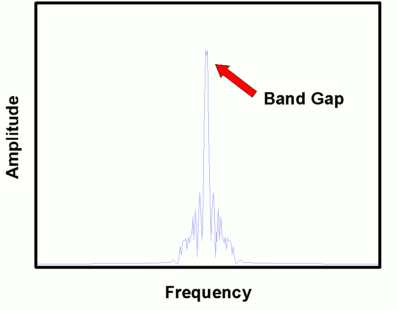 |
| Fig. 2: FDTD Simulation is one method of calculating a photonic crystal's band gap. |
Since Maxwell’s equations completely specify the behavior of light within a photonic crystal, their discretization should be sufficient to permit simulation of a given photonic crystal. Computationally, however, this is often inefficient. Often, there are means of easing the computational burden of a FDTD simulation. For instance, in the case of a two dimensional photonic crystal, Maxwell’s equations may be simplified to three update equations: two for the magnetic field and one for electric field or vice versa, depending on whether the crystal is operating in a TE or TM mode configuration. This is a tremendous improvement over the computational requirements required to update the full vector form of Maxwell’s equations. See the attached c-source for more information concerning implementation.
One also must consider the boundary conditions, which in the case of a crystal with defects should be chosen to be absorbing. This is typically accomplished by means a Mur boundary condition or a perfectly matched layer (PML). In the case of a defect-less crystal, it is generally desirable to employ Floquet boundary conditions, which ensure periodicity. See Taflove and Hagness's Computational Electrodynamics for more information. [5]
In order to discover whether a crystal has a band gap, one introduces a spatial and temporal delta function electric field into the system at a point that possesses no intrinsic symmetry. We then measure the electric field at several lattice points removed from the point of excitation, effectively finding the impulse response of the system. The Fourier transform of the impulse response effectively reveals the resonant frequencies of the system.
© 2007 R. Timp .The author grants permissino to copy, distribute and display this work in unaltered form, with attribution to the author, for noncommercial purposes only. All other rights, including commercial rights, are reserved to the author.
[1] C. T. Chan, K. M. Ho and C. M. Soukoulis, "Photonic band gaps in experimentally realizable periodic dielectric structures," Europhys. Lett. 16, 563–568 (1991).
[2] J.D. Joannopoulos, "Photonic Crystals: Molding the Flow of Light,"" (Princeton, 1995).
[3] S. Johnson, "Wave Propagation in Periodic Systems," Lecture Notes , IAP 2003.
[4] M. Maldovan, E. Thomas. "Diamond-structured Photonic Crystals," Nature Materials 3, 593 (2004).
[5] A. Taflove and S. C. Hagness, Computation Electrodynamics (Artech House, 2005).