Surface plasmon polaritons are collective longitudinal oscillations of electrons near a material surface, strongly coupled to an electromagnetic wave. The existence of coherent electron oscillations bound to the surface of a conductor were first predicted by Ritchie[1] in 1957 and demonstrated by Powell and Swan[2,3] in 1959, but have recently experienced an explosion of interest due to their ability to efficiently manipulate light on a deep sub-wavelength scale. Because the electromagnetic wave is coupled to the motion of conduction band electrons bound to the material surface, the fields are strongly localized to the surface, opening up possibilities of sub-wavelength optical detectors and waveguides; compact, sensitive chemical detectors; and enhanced light-matter interaction.
|
|
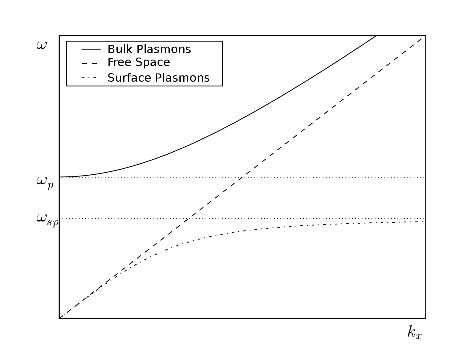
| Fig. 1: Dispersion relation for bulk plasmons, free-space electromagnetic waves, and surface plasmons. |
Both bulk and surface plasmons have associated electromagnetic waves, and can consequently be described by Maxwell's equations. The coherent oscillations of electron motion can be encapsulated in the dielectric constant of the material. The derivation of the electromagnetic fields which characterize bulk and surface plasmons is done below, and those interested are encouraged to work out the results. To keep things brief however, the basic form of the bulk and surface plasmon solutions are shown below, along with a plot of the dispersion relation for these modes.
The dispersion diagram relates the time-variation of the wave (given by its frequency &omega) to the spatial variation of the wave (given by its wave-vector kx). Bulk plasmons are associated with purely transverse electromagnetic waves, with the electric and magnetic fields perpendicular to the direction of propagation, and can only exist for &omega > &omegap (the plasma frequency). &omegap is the resonant frequency of free electrons in response to a perturbation (such as an electromagnetic field). For &omega < &omegap, the wave-vector for bulk plasmons becomes imaginary, giving an exponentially decaying wave instead of a propagating wave. It is for this reason that most metals are highly reflective for visible light (&omega < &omegap &asymp 10eV), but transparent for ultraviolet light (&omega > &omegap) [4, pg. 275].
Surface plasmons have an associated electromagnetic wave with both transverse and longitudinal field components. Such waves can only be excited at the interface between a conductor and dielectric, and are tightly bound to the surface. The fields reach their maximum at the interface (z=0), and exponentially decay away from the surface. The wave-vector of the surface plasmon mode (kspp) always lies to the right of the free space wave-vector (ko), such that &lambdaspp < &lambdao, where &lambdaspp is the wavelength of the surface plasmon and &lambdao is the wavelength of light in free space (vacuum). Additionally, this makes it impossible to directly launch a surface plasmon wave by illumination with free-space radiation: the free-space photons simply do not have enough momentum to excite the surface plasmon. As &omega increases, kspp gets larger and larger, moving further away from ko. As kspp increases, the surface plasmon wavelngth decreases and the wave is more tightly bound to the surface. This process has an upper limit of &omegasp, the surface plasmon resonant frequency, which occurs when the dielectric constant of the metal and the dielectric have the same magnitude but opposite signs.
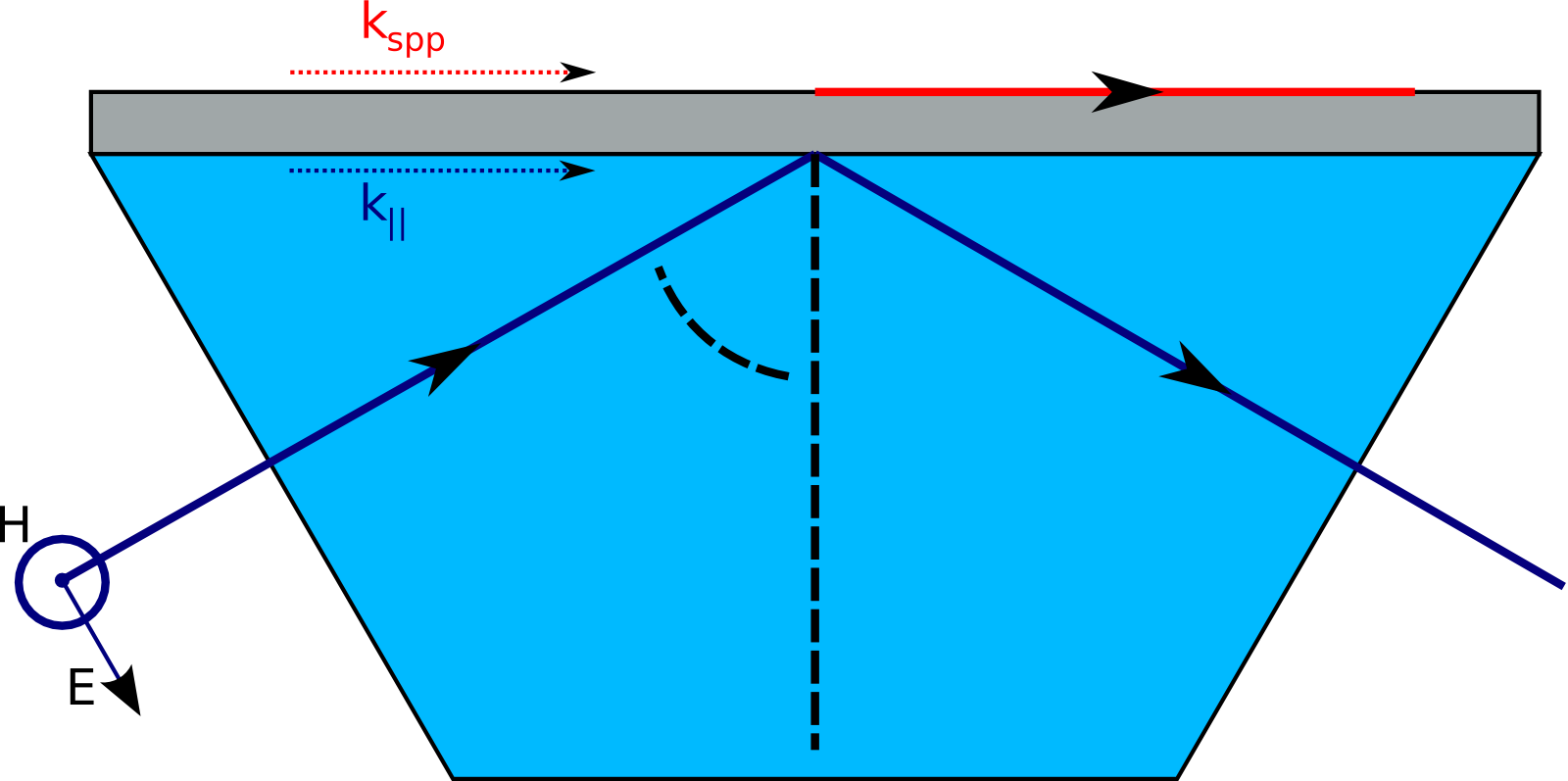 |
| Fig. 2: Schematic of a Kretschmann coupling setup for launching surface plasmons optically. |
Surface plasmons were first predicted by Ritchie[1] in 1957, and were experimentally verified by Powell and Swan[2,3] in 1959 with electron energy loss spectroscopy measurements. In these measurements, high energy electrons were used to bombard a thin metallic film and launch surface plasmons. The charge of the high energy electrons couples to the plasma oscillations of electrons in the metal; by tuning the energy and angle of incidence of the electrons, the wave-vector can be tuned and surface plasmons of a whole range of wavelengths can be excited. However, due to the high energy of the electrons, they have a very large momentum and it is difficult to precisely control the coupling: even a slight spread in energy or angle will result in a very broad range of surface plasmon wavelengths being excited. Additionally, only surface plasmons far along the dispersion curve, where kspp is largest, are generally excited. A more precise method to launch surface plasmons is through coupling with an incident electromagnetic wave (photon).
As mentioned previously, direct excitation of surface plasmons by free-space photons is not achievable because kspp is always greater than ko; this can be seen in figure 1, where the surface plasmon dispersion relation always lies to the right of the free space dispersion curve.
This can be overcome by back-side illumination through a material with a higher index of refraction (n), where the far-field radiation has a larger wave-vector (k=nko). This type of coupling geometry is shown in figure 2, and is known as a Kretschmann-Raether coupler[5]. A surface plasmon will be efficiently excited when k|| = nkosin(&theta) = kspp. Kretschmann couplers are commonly used in experiments, but are limited to very thin films such that the high-k photon is able to tunnel through the film and couple to a surface plasmon on the lower-index surface.
A more general approach to launching surface plasmons with light is the use of structured surfaces that are able to impart momentum on the photon, enabling it to couple to the surface plasmon mode. Anything from a single sub-wavelength disk or slit, to rectangular or sinusoidal diffraction gratings are used for this type of coupling. A thorough overview of surface plasmon coupling and patterned and rough surfaces is given by Raether[6].
Surface plasmons have many interesting applications such as optical measurements of films, chemicals, and biological agents bound to a metallic surface; confinement and guiding of light below the classical diffraction limit; and enhanced light-matter interaction such as surface-enhanced Raman spectroscopy (SERS). A few of the more interesting applications from the literature and industry are outlined below.
Surface plasmon resonance sensors based on Kretschmann couplers can be used to make precise optical measurements at a metal-dielectric interface. The basic idea behind these detectors is encapsulated in the coupling condition discussed above for the Kretschmann geometry: k|| = nkosin(&theta) = kspp. Since the surface plasmon is tightly bound to the metal-dielectric interface, any changes in that interface will translate directly into changes in the surface plasmon wave-vector kspp. This will cause a corresponding change in the optimal excitation angle for the Kretschmann coupler; by measuring this angle, the change in kspp can be deduced, allowing for the change in the refractive index to be computed. These detectors are sensitive enough that they can measure a change in film thickness of just a single monolayer, or refraction index changes (for example, due to chemical binding events on a bio-functionalized gold surface) as small as 10-6 RIU (refractive index units). For example, the commercial sensiQ detector from Nomadics is capable of measuring binding events of just one picogram of protein/mm2[7].
More recently, there has been an explosion of interest in surface plasmons on nanoscale patterned surfaces. Using modern nanofabrication facilities, it is possible to make structures with feature sizes much smaller than the wavelength of visible light (&sim 500nm). For example, enhanced transmission through arrays of sub-wavelength slits has been experimentally demonstrated[8] and has promising applications in photolithography and high-density optical data storage. Because surface plasmons can be launched at optical frequencies with much smaller wavelengths, it is possible to manipulate the flow of light on the scale of tens of nanometers. This has led to the coining of the term "plasmonics"[9], where surface plasmons are used to manipulate and transport information, analogous to electronics and photonics. Photonics has nearly unlimited bandwidth and almost no loss or dispersion, making it invaluable for high-throughput long-haul information networks. However, photonics components are diffraction-limited to micron-scale sizes, ruling out dense integration with nanoscale electronics. Plasmonics is potentially poised to bridge the tens of nanometer scale of modern electronics to the micron scale world of photonics. Many interesting devices, such as a 50nm metal-insulator-metal (MIM) surface plasmon waveguide capable of guiding 1.5um light[10] even around 90o corners, have been proposed and are being actively investigated. Such devices have great promise, but also must overcome the limits imposed by the lossy propagation of surface plasmons in metals. The propagation lengths of surface plasmon waves in the visible and near infrared regimes are typically on the order of hundreds of microns on unpatterned surfaces, but drop to under thirty microns in sub-wavelength MIM waveguides. The propagation length in a modern optical fiber is drastically larger, on the order of kilometers. The small propagation lengths of surface plasmons are a significant hurdle in the practical implementation of plasmonics; however, researchers throughout the world are actively pursuing geometries which take account for this loss and new designs to limit the loss as much as possible.
Surface plasmons have many exciting potential applications and rich underlying physics drawing heavily from solid-state physics and electrodynamics. Although known for over 50 years, there are still many unsolved theoretical and experimental problems in the field of surface plasmons. Additionally, with the use of modern nanofabrication techniques, a whole range of new plasmonic devices have become possible. Although not without their drawbacks, surface plasmon based devices have a plethora of laboratory and commercial applications--including the potential to revolutionize photonic-electronic integration with the burgeouning field of plasmonics.
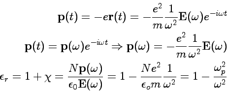
Both bulk and surface plasmons have associated electromagnetic waves, and can consequently be described by Maxwell's equations. The coherent oscillations of electron motion can be encapsulated in the dielectric constant of the material. A simple model for the motion of an electron in a conductor is a free electron driven by the field of the electromagnetic wave.
This electron motion can then be converted into a dielectric constant by using the definitions of the dipole moment, electric susceptibility, and dielectric constant[11]:
 |
| Fig. A-1: Dispersion relation for bulk plasmons and free-space electromagnetic waves. |
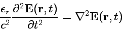
&omegap is known as the plasma frequency. This dielectric constant can then be inserted into the standard electromagnetic wave equation
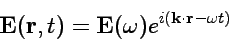
The wave equation allows for the standard propagating wave solution, given by
This is a valid solution provided that
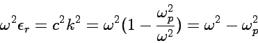
This is the dispersion relation of bulk plasmon polaritons propagating in a metallic film. The dispersion relation gives the correspondence between the time-dependence of the electromagnetic wave (&omega), and the spatial variation (k);
the wavelength of the wave is given by &lambda=2&pi/k. Figure A-1 shows a plot of the bulk plasmon dispersion relation (solid line), along with the free space dispersion relation (&omega = ck). For frequencies above the plasma frequency &omegap, the metal supports propagating modes. For frequencies below &omegap, k becomes imaginary and the fields exponentially decay inside the metal. For typical metals, h&omegap/2&pi &asymp 10eV (in the ultra-violet); for semiconductors, h&omegap/2&pi < 0.5eV (in the terahertz regime). Although bulk plasmons, which can exist even deep inside a metal, do not exist for &omega < &omegap, there is an additional solution to Maxwell's equations for these frequencies: surface plasmons.
Surface plasmons are propagating waves bound to plasmon oscillations of electrons at a metal-dielectric interface. The field intensity of the wave is at a maximum at the interface and exponentially decays away from the interface. The mathematical form of surface plasmons can be obtained by solving Maxwell's equations at a metal-dielectric interface:
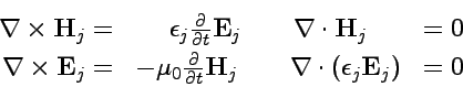
Assuming the metal-dielectric interface lies in the xy plane at z = 0, it can be shown that x-propagating surface waves of the following form are solutions to Maxwell's equations:
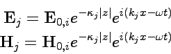
with Ex,m = Ex,d (E|| continuous), &epsilonmEz,m = &epsilondEz,d (D&perp continuous), and Hy,m = Hy,d (B|| continuous); all other field components are zero. The subscript j is used to denote fields in the metal or dielectric. The dispersion relation for surface plasmons can be obtained by inserting the equations for E and H into Maxwell's equations and enforcing the boundary conditions:
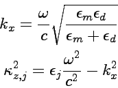
The dispersion relation, assuming &epsilonm = 1 - (&omegap/&omega)2, is shown in Fig. 1, along with the free-space and bulk plasmon dispersion relations. The surface plasmon dispersion relation always lies to the right of the free-space dispersion relations; as a result, free-space radiation does not have enough momentum to launch surface plasmons.
Additionally, the magnitude of kx for the surface plasmon asymptotically approaches &infin as &omega approaches &omegasp, where &epsilonm = -&epsilond. For &epsilonm = 1 - (&omegap/&omega)2, &omegasp = &omegap / &radic(1 + &epsilond). As kx increases, the surface plasmon wavelength decreases and &kappaz increases, resulting in a rapidly varying surface wave that is more tightly confined to the surface. For smaller values of &omega, the surface plasmon wave vector approaches the light line, the surface plasmon and free-space wavelengths become more similar, and the surface wave becomes less and less strongly confined to the surface.
For the simple free-electron model considered thus far, there is no loss in the system and the surface wave will have an infinite propagation length. In real materials, however, there is loss and the wave will only propagate a finite length. The propagation length will decrease as the surface wave becomes more tightly bound to the interface (as &omega approaches &omegasp), as the energy of the field becomes more concentrated in the metal. Consequently, there is a trade-off between confinement and propagation distance.
A final property of interest that can be obtained from the dispersion diagram shown in figure A-2 is the group velocity of the surface wave. Any information carried by the wave will propagate at the wave group velocity, vg = (&part &omega / &part k). As &omega approaches &omegasp, vg asymptotically approaches zero.
The dispersion diagram plots shown above were generated using matplotlib, an open source plotting library written in Python; the source code of the python script for the plots can be downloaded here. The images of the above equations were generated using latex and latex2html; the .tex file can be downloaded here. The figure of the Kretschmann-Raether coupler was drawn in Inkscape, an open source vector graphics editor; the svg file can be downloaded here.
© 2007 Justin White. The author grants permission to copy, distribute and display this work in unaltered form, with attribution to the author, for noncommercial purposes only. All other rights, including commercial rights, are reserved to the author.
[1] R. H. Ritchie, Phys. Rev. 106, 874 (1957).
[2] C. J. Powell and J. B. Swan, Phys. Rev. 115, 869 (1959).
[3] C. J. Powell and J. B. Swan, Phys. Rev. 116, 81 (1959).
[4] C. Kittel, Introduction to Solid State Physics, 7th ed. (Wiley, 1995).
[5] E. Kretschmann, Z. Phys. 241, 313 (1971),
[6] H. Raether, Surface Plasmons on Smooth and Rough Surfaces and on Gratings (Springer, 1988), pp 1-133.
[8] T.W. Ebessen et. al, Nature 391, 667 (1998).[9] S.A. Maier et. al, Adv. Mat. 13, 1501 (2001).
[10] G. Veronis and S. Fan, Appl. Phys. Lett. 87, 131102 (2005).
[11] J. D. Jackson, Classical Electrodynamics, 3rd ed. (Wiley, 1998).