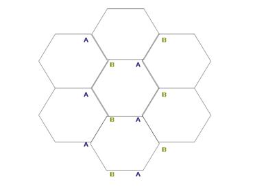
Graphite is a 3D crystallographic form of carbon material, which has been known to humans for ages. Over the past decades, researchers have discovered the fullerenes [1], a 0D form of carbon and the carbon nanotubes [2], a 1D form of carbon. All these materials can be viewed as derivatives of a single building block – a 2D sheet of carbon, a few angstrom thick, arranged in a honey comb lattice called graphene (fig 1). Graphite consists of many graphene layers, weakly connected by Van der Waals’ forces, while fullerenes and nanotubes can be viewed as 2D sheets rolled in a certain way (either a buckyball or a nanotube). Although graphite was extensively investigated theoretically over numerous decades, this type of material, which is only one atom layer thick, has only been discovered a few years ago [3]. Prior to its discovery, failures to isolate the single 2D layer were attributed to the Mermin-Wagner theorem, which states that a real 2D material cannot exist due to instability considerations. However, the discovery of graphene does not contradict the Mermin-Wagner theorem since graphene is either placed on another substrate or for free hanging graphene, it has ripples which cause it to curve[4].
|
|
| Fig 1: The Honeycomb Lattice of Graphene consists of two equivalent sublattices from sites A and B. Each site is a carbon atom. |
The bands structure of graphene was calculated by Wallace in 1947 [5]. The two equivalent carbon sites, denoted by A and B in Fig. 1, produce the two bands - pi and pi* - which intersect in two inequivalent points in the First Brillouin zone Zone, K and K', justifying the name "gapless semi-metal" for graphene. These two points are called the Dirac points, and close to these points, within the low-energy excitations, the dispersion relation is linear (Fig. 2). This conical shape of the dispersion relation is the analog of the dispersion relation of a photon, with the Fermi velocity in graphene (300 times smaller than the speed of light), taking the role of the speed of light. Thus, although the electrons in graphene are not relativistic particles, the equations that govern their motion are very similar to those of massless relativistic particles. As such, the transport properties of graphene are quite different from other metals and semiconductors, where the dispersion relation can be approximated by a parabola. Those differences manifest in the unusual quantum Hall effect in graphene that was already confirmed experimentally [6] (and will not be described here), and by the possibility of observing the Klein Paradox in a condensed matter experiment setup [3,7]. In addition, the conical nature of the dispersion relation is a consequence of the symmetry between electron type carriers and hole type carriers in graphene (fig 2). This symmetry, which stems from the symmetry of the two equivalent points in the lattice, is important for the understanding of the Klein Paradox, as will be described below.
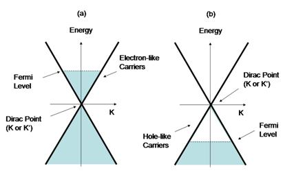 |
| Fig 2: The linear dispersion relation of electrons in graphene at the ends of the 1st Brillouin Zone. This conical shape is the same at K and K' points. (a) When the Fermi level is above the Dirac point the carriers are electron-like (b) When the Fermi level is below the Dirac point, the carriers are hole-like. |
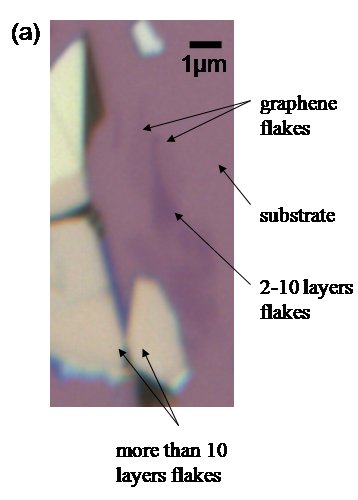
There are several ways of making graphene sheets. The most common ones are the mechanical cleaving [8] and the epitaxial growth [9]. The former is by far the easiest way, while the later will probably become the commercial way of mass production of graphene flakes. Micromechanical cleaving typically produces graphene sheets of up to tenths of microns with mobilities of up to 20,000 cm2/(V*sec). The mechanical cleaving technique uses either HOPG (Highly Oriented Pyrolytic Graphite) crystals or natural graphite, which are spread on top of a scotch tape. Then after repeatedly folding and unfolding the tape several times, one can deposit flakes of different thicknesses on top of silicon substrate, which was already oxidized (SiO2) on the surface to 300nm (this thickness is chosen to make it easier to identify a single flake and to create a back gate for the final device). Using optical microscope, one can identify single layer flakes by their color, where each number of layers has a different color due to the different path the light has to travel (Fig. 3). After finding a single layer flake, one can design the pattern of the leads by electron beam lithography and evaporation of titanium and gold. Once the sample is wired, the device is ready for transport measurements. The common measurements are 2-probe and 4-probe measurements in low temperatures (down to a few tens of milikelvin in a dilution fridge), and fields up to 10 Tesla.
The quantum description of a non relativistic electron allows it to tunnel through a barrier. The tunneling probability decreases exponentially with the height and width of the barrier. Counter-intuitively, for a relativistic electron, the tunneling probability through a barrier can be close to unity when the barrier is higher than twice the rest mass of the particle (in units of energy). More surprising is the fact that the higher the barrier, the closer the probability is to unity, together with a weak dependence on the barrier width. This phenomenon is called the Klein Paradox [10], and can be explained by the fact that although the barrier is repelling for electrons, it attracts positrons (or in the case of graphene- holes). This way the positrons energy states can be aligned to the electron states, which leads to high probability of tunneling through the barrier. For electrons in graphene, which behave as massless relativistic particles, one can show that the probability of tunneling though the barrier, when the electrons are perpendicular to the barrier, is close to unity [7]. Thus, experiments on graphene can be used as reachable and convenient setup, for testing the Klein Paradox, and shed light on the fundamentals of quantum physics, which otherwise in real relativistic systems is impractical to implement.
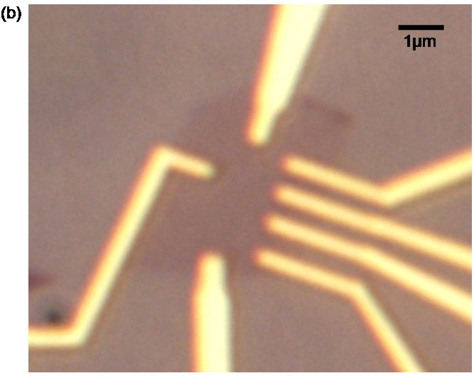 |
| Fig 3: (a) Optical microscope picture. The single layer graphene flakes has almost the same color as the substrate, while the graphite flakes are easily spotted. (b) Simple device - gold leads area attached to a graphene-like sample. |
© 2007 N. Stander. The author grants permission to copy, distribute and display this work in unaltered form, with attribution to the author, for noncommercial purposes only. All other rights, including commercial rights, are reserved to the author.
[1] R.F. Curl, Rev. Mod. Phys. 69, 69 (1997).
[2] S. Iijima, Nature 354, 56 (1991).
[3] K.S. Novoselov et al., Proc. Natl. Acad. Sci. 102, 10451 (2005).
[5] P.R. Wallace, Phys. Rev. 71, 622 (1947).
[6] K.S. Novoselov et al., Nature 438, 197 (2005).
[7] M.I. Katsnelson, K.S. Novoselov, and A.K. Geim, Nature Phys. 2, 620 (2006).
[8] Y. Zhang, Y.-W. Tan, H.L. Stormer, and P. Kim, Nature 438, 201 (2005).
[9] C.Berger et al., J.Phys. Chem. B 108, 19912 (2004).
[10] O. Klein, Z. Phys. 53, 157 (1929).