A Review of Scanning Electron Microscopy with Spin
Analysis
J. Bert
March 7, 2007
(Submitted as coursework for Applied Physics 272, Stanford
University, Winter 2007)
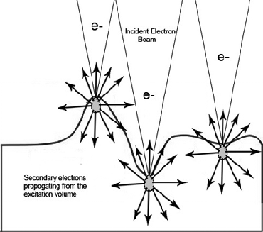 |
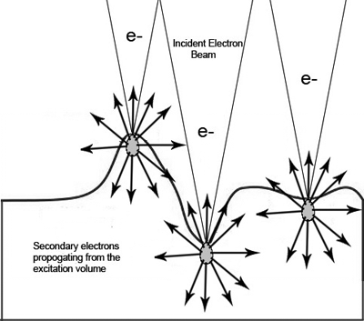
| Fig. 1: The incident electron beam excites an
electron cascade that spreads out into a volume in the
sample shown in gray. Excited secondary electrons,
represented by the black arrows spread out from the
excited volume. The number that escape depend on the
curvature of the sample. |
|
 |
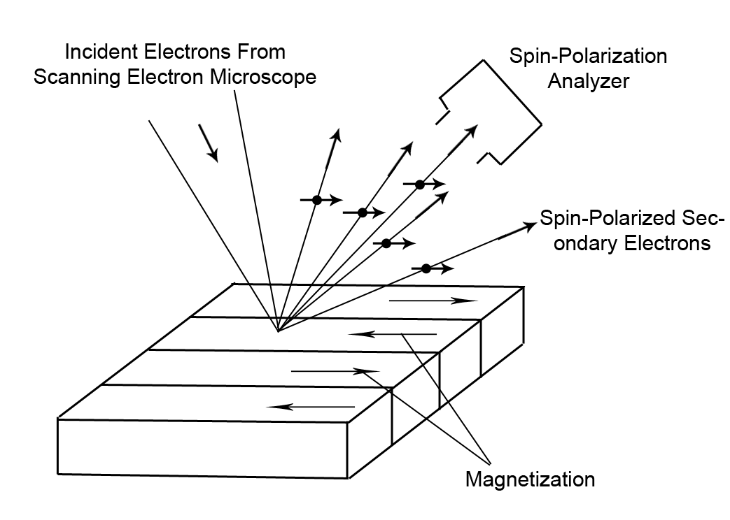
| Fig. 2: This schematic shows basic idea behind
the SEM with spin analysis. Incident electrons excite
secondaries which maintain their polarization. The
polarization is then read out by a spin analyzer.
Figure redrawn from Allenspach.[2] |
|
Scanning electron microscopy with spin analysis
(SEMPA) has created new opportunities to study the orientation and
structure of magnetic domains, domain walls and magnetic singularities
in materials. All of these structures are extremely complex and a best
studied through direct observation.
SEMPA is a refinement to the well established
scanning electron microscopes or SEM. The SEM has long been used to map
the surface of materials at resolutions better than the diffraction
limit of light. An SEM probes a surface with a highly focused beam of
high energy electrons (<10 keV). When the highly energetic electrons
hits the surface they inelastically scatter off the valence electrons in
the material. Each interaction between the incident electron and a
valence electron excites the valence electron and slightly reduces the
energy of the primary electron. Both the incident electron and the
valence electron go on to collide with other valence electrons, creating
a cascade of excited valence electrons know as secondary electrons. Some
of these secondary electrons propagate back to the surface where they
can escape into the vacuum. The number of secondary electrons that
escape is highly dependent on the topography of the surface.
As is demonstrated in figure 1 the volume of excited
secondaries remains constant; however, in regions with greater surface
curvature more of the excited volume is close to the surface and
therefore more secondaries are able to escape. By collecting the
secondary electrons generated and plotting the intensity as a function
of probe position one can make a reliable map of the surface
topography.
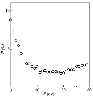 |
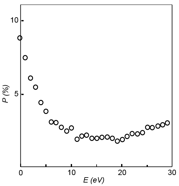
| Fig. 3: The polarization of secondary electrons
vs. kinetic energy of secondary electrons from samples
of Ni(100). Notice the much higher polarization at
lower energies. A possible cause of the enhanced
polarization is selective scattering of the minority
spin electrons at low energies. Figure redrawn. Data
from Allenspach.[2] |
|
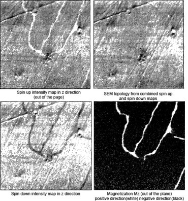 |
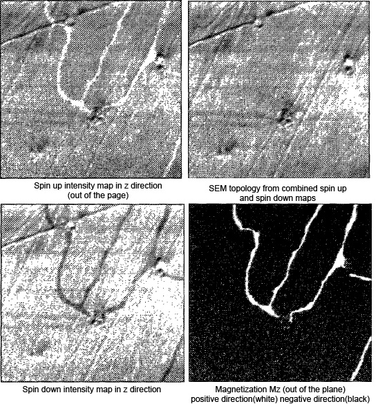
| Fig. 4: The four images here all represent
intensity signals from the analysis of the z component
(directed out of the page) of the sample
magnetization. The spin up intensity is the number of
spin-up electrons detected, N↑ (upper
left). The spin down intensity is just
N↓ (lower left). The topographical map
is the total intensity
N↑+N↓ (upper right),
and the polarization map is found using
(N↑-N↓)/(N↑+N↓)
(lower right). Data from Allenspach.[2] |
|
An SEM maps the topography of a sample but does not
probe the magnetic properties of a sample. However, the secondary
electrons ejected from a sample maintain their polarization.[1]
Secondary electrons in a magnetic material are polarized antiparallel to
the magnetization vector of the domain they originate from. By
measuring the average spin polarization of the emitted secondary
electrons the polarization of the material is revealed. Polarization
can be calculated from the ratio of the spin differential to the total
number of spins.

N↑ is the number of electrons with
spin-up and N↓ is the number of electrons with spin
down.
Secondary electrons excited from the valence band maintain their
polarization after escaping the surface; however, to get an accurate
measurement of the magnetization of domains in the sample the
secondary electrons must maintain their polarization until they
reach the spin analyzer. To maintain coherent polarization the
apparatus must be shielded from stray magnetic fields and the sample
surface must be clean and free from impurities that may cause
spin-flip scattering. As a result measurements must take place in
UHV with an ambient pressure of less than 10-9 Torr.
[3] In addition, to ensure a clean surfaces,
samples must be prepared and/or cleaned in situ using a sputter ion
gun and an Augar electron spectrometer for characterization of the
cleaned sample.
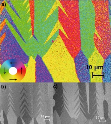 |
| Fig. 5: a)Map of the angle of the in-plane
magnetization of Fe. Map is derived from a combination of
the map Mx in figure (b) and the map of
My in figure (c). The color wheel gives the
relationship between color and direction.[11]
|
After samples are prepared, a focused beam of
primary electrons is used to probe the sample. The beam can be
characterized by it's energy, current and diameter on the sample
surface. Each parameter must be optimized to assure the best signal to
noise and resolution in the final image. Secondary electron yield is
highly dependent on incident beam energy. Lower energy beams excite
many more secondaries, but very low energy beams can be deflected by the
extraction field used to bring ejected secondaries to the spin analyzer.
In practice the energy of the primary electrons must be at least 10
KeV.[3] The probe current and diameter are related. Increasing the probe
current increases the area on the sample that will be excited by the
probe. Better resolution demands smaller probe diameters, which limits
the magnitude of the current. Smaller probes with higher resolution
require low probe currents. Low probe currents are more susceptible to
quantum noise. As a result scans with low probe currents require longer
dwell times to increase the signal to noise ration, which therefore
increases the amount of time required to scan a sample. An upper limit
for the time for a scan is set by drift and deterioration of the sample.
All these factors place a practical limit on the expected resolution of
a SEMPA system at 10 nm.[4] SEMPA resolutions are quickly approaching
that limit, to date the best resolution has been reported to be 20 nm by
Matsuyama and Koike.[5]
The polarization of secondary electrons that escape
from the sample is dependent on the magnetization of the domain it came
from in the sample, but if the sample is a 3d ferromagnet it also
exhibits a strong dependence on the secondary electron
energy.[1][6][7]
As show in Figure 3 the polarization of Ni is
artificially enhanced at lower energies. The the bulk magnetization of
the domains in the material match the polarization of higher energy
secondary electrons, therefore a minimum cutoff of 10 eV is applied to
the electrons that are spin analyzed.[2][8]
The origin of the low energy enhancement to the
polarization has not been fully explained, however one plausible
explanation argues the enhancement at low energies is caused by
selective scattering of minority spin electrons, which further
exacerbates the spin differential to make the majority spins even more
dominant. Selective scattering occurs, in 3d ferromagnets, where the
valence band in filled with spins predominantly oriented in the same
direction (spin up in this example). Inelastic scattering only occurs
between electrons of opposite spin. From Pauli's exclusion principle
Coulomb interactions between electrons with identical spin will be
canceled by exchange.[9] It follows that the minority spin electrons
will have a shorter inelastic mean free path and are therefore less
likely to escape from the sample. This asymmetry in the inelastic mean
free path decreases with increasing electron energies.
A hemispherical energy analyzer is used to eliminate
low energy electrons and secondary electrons with energy greater than 10
eV are transported to a spin analyzer. Mott detectors are the most
commonly used spin analyzers, however low-energy electron diffraction
(LEED) analyzers, absorbed current analyzers and low-energy diffuse
scattering (LEDS) analyzers have also been used. A Mott detector
exploits the spin-orbit coupling of the electrons to convert spin
differences into measurable spatial differences. Electrons are
accelerated and scattered off a thin film of a material with a large
atomic number, usually gold. The interaction of the spin of the
electrons with the gold atoms causes different spins to scatter in
different directions. The spin-orbit interaction is sensitive to
electrons whose spin is parallel to the plane of the foil. For example,
if the gold foil were oriented in the xy-plane, electrons with
Sx↑ would be scattered to the right, electrons with
Sx↓ would be scattered to the left, electrons with
Sy↑ would be scattered up and electrons with
Sy↓ would be scattered down. The scattered electrons
detected by a group of four electron detectors placed symmetrically
about the incident beam.
A single analyzer can measure the two polarization
components simultaneously. To measure all three components, a second
analyzer is necessary. The incident electrons beam is split to send
half of the electrons to each of the two analyzers. The analyzers
measure two independent components and one common component which can be
used to calibrate the analyzers with respect to each other. The
magnetization of magnetic domains within the sample can then be
determine by calculating the polarization from equation (1) Topological
information can be concurrently recorded as a normal SEM image by
mapping the sum of all the electrons collected.
Once the polarization of the secondary electrons is
calculated an image of the magnetic domains can be created by mapping
different polarization directions to different colors. Figures 4 and 5
are just some examples of the type of images an SEMPA can capture.
Figure 4 is an ultrathin Fe sample epitaxially grown
the (100) surface of Cu. The images clearly demonstrates one of the
great strengths of the SEMPA technique: the ability to separate the
topographical signal from the magnetic signal. The topography is evident
in the total intensity map, as well as the individual spin intensity
maps. However, the polarization map shows no evidence of the sample
topography. The topography and magnetization have been separately
measured.
A second example of what the SEMPA is capable of is
shown in Figure 5. It maps the domains of a Fe whisker and was captured
by the Danish company Omicron NanoTechnology GmbH with their commercial
SEMPA. With a resolution of about 10 nm it represents the state of the
art in SEMPA detectors at the limit of spatial resolution.
These examples are meant to be illustrative, not
exhaustive, and highlight some of the benefits of the SEMPA technique.
In addition to the high resolution and the separation of the
magnetization and the surface topography, other benefits of the SEMPA
system include the ability to measure many types of samples from bulk to
thin films, and scan over large areas. Drawback of the SEMPA system
include a predicted resolution threshold of 10 nm, required UHV
conditions for measurement and sample preparation, and long scan times
necessary to reduce noise created by low yields of secondary electrons
and low detector efficiencies. Despite these drawbacks the SEMPA
systems is well suited to studying magnetic domain at very high
resolutions, and will continue to play an important role in magnetic
imaging.
© 2007 J. Bert. The author grants permission
to copy, distribute and display this work in unaltered form, with
attribution to the author, for noncommercial purposes only. All other
rights, including commercial rights, are reserved to the author.
References
[1] J. Unguris, D. Pierce, A. Galejs, and R. Celotta,
Phys. Rev. Lett. 49, 72 (1982).
[2] R. Allenspach, IBM Journal of research and
development 44, 553 (2000).
[3] M. Scheinfein, J. Unguris, M. Kelley, D. Pierce,
and R. Celotta, Rev. Sci. Inst. 61, 2501 (1990).
[4] E. Dahlberg and R. Proksch, J. of Mag.
Mag. Mat. 200, 720 (1999).
[5] H. Matsuyama and K. Koike, J. Electron Microsc.
43, 157 (1994).
[6] E. Kisker, W. Gudat, and K. Schröder, Solid
State Comm. 44, 623 (1982).
[7] H. Hopster, R. Rave, E. Kisker, G. Guntherodt,
and M. Campagna, Phys. Rev. Lett. 50, 70 (1983).
[8] D. Abraham and H. Hopster, Phys. Rev. Lett.
58, 1352 (1987).
[9] X. Sun, Z. Ding, and Y. Yamauchi, Surface and
Interface Analysis 38, 668 (2006).
[10] K. Koike, H. Matsuyama, and K. Hayakawa,
Scanning Microsc. Intern. Suppl. 1, 241 (1987).
[11] G. Schäfer, Omicron Nanotechnology Website
(2007/03/05), http://www.omicron.de